Samsung chip facility opens in Xi'an
By Lu Hongyan and Ma Lie in Xi'an (China Daily) Updated: 2014-05-10 07:19
 |
|
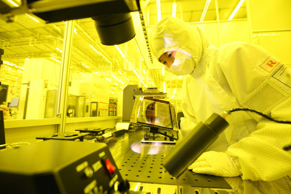
A Samsung Electronics Ltd memory chip project that cost $7 billion began operations on Friday in the Xi'an Hi-tech Development Zone in Shaanxi province.The project has about 230,000 square meters of floor space for the production of 10-nanometer NAND flash memory chips. Provided to China Daily |
Plant is one of three major production bases in world for South Korean giant
A Samsung Electronics Ltd memory chip project that cost $7 billion began operations on Friday in the Xi'an Hi-tech Development Zone in Shaanxi province.
The project has about 230,000 square meters of floor space for the production of 10-nanometer NAND flash memory chips.
NAND stands for Not And Hard Drives, which are high-capacity, high-speed devices.
|
 |
|
 |
Samsung plans to complete the construction of a semiconductor packaging and testing plant by the end of 2014 to build a complete semiconductor production chain.
Annual sales are estimated at 60 billion yuan ($9.63 billion) at full production levels.
With the official opening of the project, Samsung has created a global semiconductor production system with three major production bases, one each in South Korea (systems and storage semiconductors), China (storage semiconductors) and the United States (systems semiconductors), Kwon said.
Samsung signed a strategic agreement for the project with Shaanxi province on April 10, 2012 and construction began on Sept 12, 2012.
The investment of $7 billion, which covers just the first phase of the facility, makes it the largest single foreign-invested project in China so far.
Samsung said that it chose Xi'an because of the city's excellent investment environment and services, as well as its fast-developing electronics industry, a deep pool of researchers and a well-trained labor force from more than 100 research institutes and universities.
Qiao Minwei, a university student in the city, said that he and his classmates welcomed the project, which offers a chance for employment.
 |
 |
| Samsung-Apple battle enters second round |
|
- Cabinet calls for new share listing system
- China levies anti-dumping duties on pipes
- China's auto output, sales down from record high
- Samsung launches full-scale chip production in China plant
- Time to enhance protection for overseas Chinese firms
- Oil trade show concludes with heavy Chinese presence
- China, Russia vow to increase two-way investment
- China, Angola to deepen economic ties: minister


