JCET hits significant high-tech microchip milestone
By Ma Si | China Daily | Updated: 2023-01-11 09:13


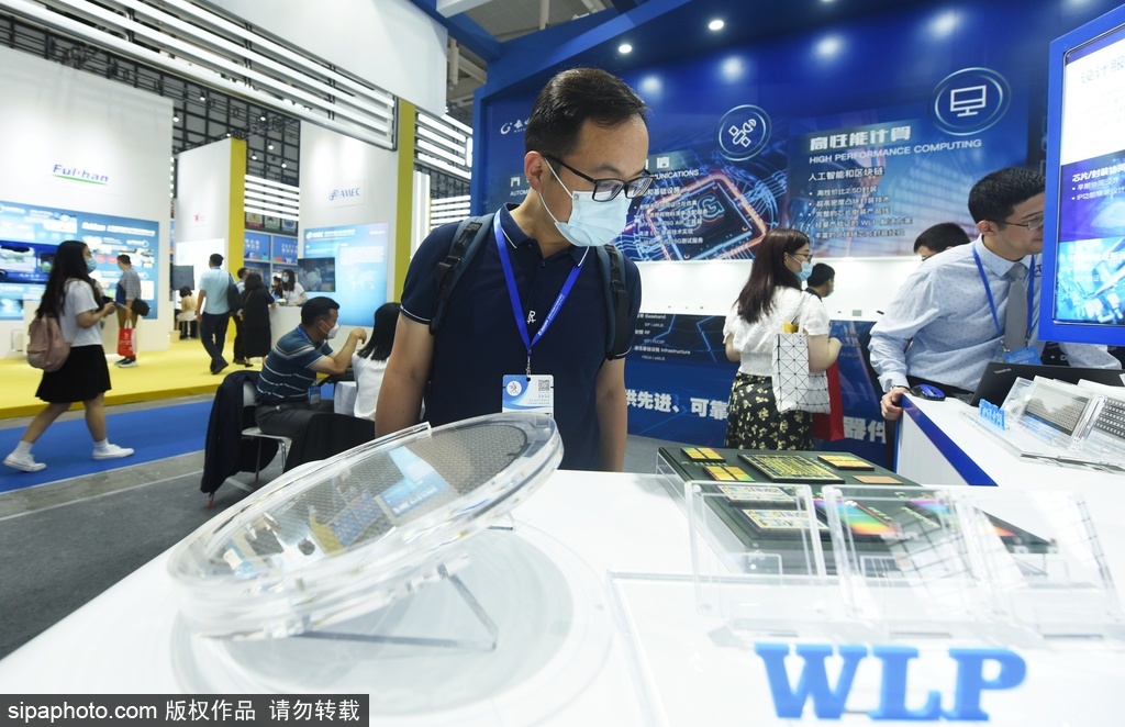
JCET Group, a leading Chinese provider of integrated circuit back end manufacturing and technology services, said it has achieved high-volume manufacturing of integrated packaging for 4-nanometer chips.
This marks a breakthrough in the country's chip packaging industry, and represents the progress local companies have made with hard work, experts said.
Packaging is an essential part of semiconductor manufacturing and design. It affects power, performance and costs on a macro level, as well as core functionality.
JCET said it has leveraged chiplet technologies to achieve production of packaging for 4 nm chips for foreign customers, with a maximum packaging area of some 1,500 square millimeters.
Chiplet is essentially a technology that allows an integrated circuit block to be interconnected with other ICs to form a larger, more complex chip.
With the rapid development of high-performance computing, artificial intelligence, 5G, smart automobiles, cloud and other applications in recent years, continuous innovation of back-end manufacturing technologies is required to compensate for the slowdown of Moore's Law, JCET said on its official website.
Moore's Law is a key rule that has affected the integrated circuit sector for a long time. It states that roughly every two years, the number of transistors on a microchip will double.
In response to market demand, JCET is working hard to explore new, advanced chip packaging technologies, the company said.
Wu Jiangxing, an academician at the Chinese Academy of Engineering, said chip manufacturing is evolving to embrace more difficult designs and complicated processing. This in turn is causing costs to continue to rise.
Against such a backdrop, chiplets are rising in importance as they can improve productivity and yields, lower design complexity and help cut costs of both design and manufacturing, experts said.
A Zheshang Securities report expressed a similar view, noting that as an important alternative to conventional chips, chiplets may bring new opportunities to the domestic semiconductor industrial chain.
Founded in 1972, JCET's comprehensive portfolio covers a wide spectrum of semiconductor applications such as smartphones, communications, computing and automobile, through advanced wafer-level packaging.
JCET has two research and development centers in China and South Korea, six manufacturing locations in China, South Korea and Singapore, and sales centers around the world.
Related Stories


Editor's Pick